Before coming into my office, please turn your cell phone off.
The textbook "Design with Operational Amplifiers" by Sergio Franco is available in a much cheaper softcover international edition. Some of the cites selling this edition are listed at AbeBooks.com. To my knowledge, these books cannot be "sold back" to the Georgia Tech bookstore.
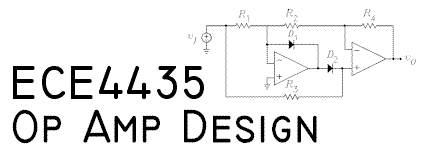
Circuit diagrams of operational amplifiers:
LM741 A workhourse general purpose op amp for many years. Not the best for new designs requiring high performance.
TL071 An example of a high performance general purpose op amp.
uA749 This is a very old op amp and is no longer made.
Click here to read a paper on the application of superposition to circuits containing controlled sources. The circuits courses say that you can't, but you can.
Here, here, and here are good tutorials on strain gauges.
Supplementary Class Notes - Chapter 1
Supplementary Class Notes - Chapter 2
LTSpice is distributed by Linear Technology and has become the defacto standard for the "do it yourself" electronics and audio communities. Unlike other free versions, there are no limits on the number of devices in a circuit. Here are the links:
Linear Technology Software Page
LTSpice Tutorial
LTSpice Guide
The GTA for the class is James Barfield. His hours in the Tutotial Lab are Thursday from 9:00 am to noon. His email address is jbarfield3_at_gatech_dot_edu.
Project I - A Wien-bridge Oscillator
Project II - An Intermodulation Distortion Analyzer
Project III - The Class-D Amplifier
Project IV
The compressor amplifier described in class is an advanced circuit that could take a lot of tweaking time in the lab. For this reason, you are given the option between the compressor experiment and a simplier experiment that illustrates how feedback linearizes the output stage of an audio amplifier. If you like experimenting with analog circuits, you should do the compressor experiment. If you wish to do an experiment that will require little tweaking, you should do the optional experiment. A description of the compressor amplifier is here. The LTSpice file is here. The optional experiment is here.
Here is the LTSpice file for an improvement to the original compressor amplifier posted above. It involves the addition of one resistor, one capacitor, and two diodes. In addition, the values of some elements are changed and the gain of E2 has been changed from 40 to 20. The addition of R10 allows adjusting the threshold of compression. The value in the file sets it at about 1 V whereas it was about 400 mV for the original circuit. The addition of diodes D5 and D6 in the integrator is necessary to make the adjustable threshold work. E5 has been changed to a non-inverting amplifier and the directions of D3 and D4 are reversed. Figure 2.23 in the text shows a 2 op-amp instrumentation amplifier which can be used for E5 if desired.
Assignment 1
PDF scan of Chapter 1 problems.
Problem 1.15
Set v_O - 4 = v_P to solve for v_O
Problem 1.16
For part (a) the 3k and 2k resistors have no effect on the answer. For part (b) make a Thévenin equivalent circuit, or use current division to solve for the fraction of the source current that flows in the original resistors of the circuit. (The latter is the easiest, just remember that the op amp has a virtual short between its inputs when using current division.)
Problem 1.18
Calculate v_P and v_N in terms of v_O and solve for v_O. For part (b) make a Thévenin equivalent circuit.
Problem 1.21
With the switch closed, v_P = 0. Use the gain formula for the inverting amplifier to solve for v_O. With the switch open, divide the source v_I into two equal parallel sources, one connected to R_1 and the other connected to R_3. Erase the lead that connects the two sources. There is no drop across R_3 so that v_P = v_I. Use superposition of the two input sources, the non-inverting gain formula, and the inverting gain formula to solve for v_O. Repeat the same procedure with the added resistor. You only need the inverting and non-inverting gain formulas to write the answer by inspection.
Problem 1.22
Calculate v_P in terms of v_I using voltage division for the voltage divider formed by kR_3 and (1-k)R_3. Use superposition of v_I and v_P to solve for v_O.
Problem 1.24
Solve for the output voltage of OA_2 in terms of v_O. Use this to solve for v_P for OA_1 and set this equal to v_I.
Assignment 2
Problem 1.31
For the vN inputs, use the inverting gain formula and superposition for v1, v3, and v5 to solve for vO. For the vP inputs, make Norton equivalents of the 3 sources connected to the vP input to obtain 3 current sources in parallel with a single resistor. Solve for vP and use the non-inverting gain formula to solve for vO.
Problem 1.43
Let vI be the input voltage and vO be the op-amp output voltage. At the vP node, make a Norton equivalent of [vI,R1] and [vO,R2]. Use the circuit obtained to write the equation for vP. Use voltage division to solve for vN. Set vP = vN and solve for vO. Use the value of vO to solve for vN. Set vP = vN to obtain an equation for vP in terms of vI alone. Calculate the input current iI by dividing the voltage across R1 by R1. Calculate the input resistance by dividing the input current by vI. The vI should cancel from the equation.
Problem 1.44
Use the inverting amp equation to solve for vO as a function of vI. The answer is independent of the second op amp and the resistors connected to it. Use the inverting amp equation to solve for vO2 as a function of vO. Use the two equations to solve for vO2 as a function of vI. Use the equations to calculate the currents through R1 and R3 as functions of vI alone. Sum the currents to solve for the input current. Divide vI by the input current to get the input resistance. The vI should cancel out.
Problem 2.5
Let v3 be the voltage across R3. Solve for the currents into the vN node in terms of vI and v3. Solve the equation for v3 as a function of vI. Solve for the currents through R2 and R3 and take their difference to get iO.
Problem 2.9
At the vL (vP) node, make Norton equivalents of [v2,R1] and [vO,R2]. Use the circuit obtained to write the equation for vL in terms of v2 and vO. Solve the equation for vL. At the vN node, make Norton equivalents of [v1,R3] and [vO,R4]. Use the circuit to write the equation for vN. Set the equations for vN and vL equal to each other and solve the equation for vO as a function of v1, v2, and iO. Now use the equation for v_O in the first equation for v_L and solve the equation obtained for iO as a function of v1, v2, and vL. To obtain the condition that iO be independent of vL, set the coefficient of vL equal to zero. This makes the circuit a perfect current source.
Problem 2.14
Make Norton equivalent circuits at the vP11 node and write the equation for vP11 as a function of v2 and vL = vO2. Use superposition of v1 and vP11 to solve for vO1 as a function of v1, v2, and vL. Set this voltage equal to vL + iO x R5. Solve this equation for iO as a function of v1, v2, and vL. Use the equation to solve for the conditon that iL be independent of vL. This is the condition that the circuit act as a perfect current source.
Assignment 3
Problem 2.15
Use superposition of vI and vO2 to solve for vO1. Set vL = vO1 and vO2 = vL + iO x R5. Use the equation to solve for iL as a function of vI and vL. Use the equation to solve for the conditon that iL be independent of vL. This is the condition that the circuit act as a perfect current source.
Problem 2.16
Solve for vO2 as a function of vI and vL. Set this equal to (IL + vL/R2) x R3. Use the equation to solve for iL as a function of vI and vL. Use the equation to solve for the conditon that iL be independent of vL. This is the condition that the circuit act as a perfect current source.
Problem 2.21
Use superposition to solve for vP as a function of iS and vL. Set vN = vP. Calculate iL as (vP - vL)(1/R1 + R2). Use this equation to solve for iL as a function of iS and vL. The equation should be of the form iL = AI x vS - vL/RO, where RO is the output resistance.
Problem 2.25
Use the inverting gain formulas and superposition to write the answer by inspection. I think the figure should have been drawn with vP1 grounded and R connected from vO1 to vN2. You get the same answer either way.
Problem 2.39
This is tricky because you cannot use the inverting or non-inverting gain formulas for OA1 because it does not have negative feedback. However, the overall feedback is negative because OA2 inverts the signal that is fed back to OA1. Thus a virtual short between v1 and vP1 can be assumed. Why one would use this circuit, I do not know, but it is a good problem to practice superposition. You can also use node equations. First set vP1 = v1 and vN2 = v2. Use superposition and the inverting and non-inverting formulas to write vO2 as a function of v1, v2, and vO. Set vN2 = v2. Use superposition of v2 and vO2 to write the equation for vP1. Set this equal to v1. Eliminate vO1 between the equations and solve for vO as a function of v1 and v2.
Problem 2.52
Use superposition of VREF and vO to solve for vN. Use voltage division to solve for vP. Equate the two and solve for vO.
Problem 2.54
Use the inverting gain formula to solve for vO1 as a function of VREF. Use superposition of VREF and vO1 to solve for vO. The figure in some books might have the (1 + δ) term on the wrong resistor. Note that someone holds a patent on this simple little circuit.
Assignment 4
Problem 3.7
The zero-pole name does not mean that there are no poles. It means that the circuit has a zero and a pole and that the zero occurs at the lower frequency on the Bode plot. Another name is a lead-lag circuit. The zero provides phase lead and the pole provides phase lag.
Problem 3.8
The simplest way to do this problem is to replace the source with 2 equal sources connected to two separate inputs. Then use superposition between the 2 sources to obtain the output voltage.
Problem 3.15
Note that the input capacitance connects to ground.
Problem 3.16
As in the preceding problem, the capacitance connects to ground. To solve for it, solve for the ratio of V to I at the input.
Problem 3.21
Click here to download the 5 cycle log-log paper for the plots. Note that this is not dB-log paper. You plot the gain on the vertical axis, not 20log(gain).
Problem 3.22
Problem 3.25
Problem 3.26
Assignment 5
Problem 3.27
Write node equations at the upper nodes of C1 and C2. Use the inverting op-amp gain formula for V_o.
Problem 3.28
Write a node equation at the node to the right of R1. Use the inverting op-amp gain formula for V_o.
Problem 3.33
Use superposition of Vi and Vo to solve for Vo1. Use the transfer function of the BPF to write Vo as a function of Vo1. The Vo will be on both sides of the equal sign. Solve for Vo.
Problem 3.37
Replace Vi, R, and mR with a Thévenin equivlent circuit consisting of one source in series with one resistor. Use superposition to solve for VBP as a function of Vi and VLP. Write VLP as a function of VBP. VLP will be on both sides of the equal sign. Solve for VBP. Solve for VLP. Solve for VBP.
Problem 3.38
Use the solutions for the non-inverting state-variable filter that were obtained in class.
Part One
The Class-D Amplifier. The linked document explains the theory of operation of the class-D amplifier and gives some of the design equtions. The object of this project is to design a mock class-D amplifier with op amps, comparators, and complementary MOS transistors. Do not use the 741 op amp for any of the circuits. It has too low a slew rate to be used in this project.
The first step is to assemble the triangle wave generator using an op amp in place of the comparator. The design of this circuit is covered in the course textbook. Design the circuit for an initial 50kHz triangle-wave frequency. The peak voltage of the triangle wave is to be 10V. This voltage sets the clipping voltage of the class-D amplifier at 10V. If you cannot get the triangle wave generator to work properly at 50kHz, it may be necessary to lower its frequency. However, the class-D amplifier requires this frequency to be as high as possible.
The second step is to connect the triangle wave and the test signal from a function generator to the two inputs of an op amp that is used as a comparator. You should see an output that looks like a square wave with a modulation of the widths of its positive and negative peaks. If the op-amp comparator will not switch at 50kHz, it may be necessary to reduce the triangle wave frequency.
An IC chip containing the MOS transistors for the CMOS inverter will be provided in the lab. The third step is to connect this to the output of the op-amp comparator. The inverter may not switch properly without a resistive load on it, so it might be necessary to connect a resistor from its output to ground. You might try a 10kohm resistor. The value may have to be reduced for the circuit to work properly.
In the first lab, you should be able to get the basic circuit to work using op amps for the comparators.
Part B
Until I can see if I can make the CMOS inverter output stage work, you can omit it from the circuit. I will try to see if I can make it work properly this afternoon (Jan. 22). If I can, you can add it to the last part of the experiment next week.
The object this week is to design an active filter to recover the audio signal from the pulse-width modulated signal output of the comparator. The document linked in Part One that describes the class-D amplifier shows a passive 2nd-order LC filter for this. Although a passive filter must be used if the amplifier is to drive a loudspeaker, we can replace it with an active filter for purposes of this lab. The filter is to be a 3rd-order Chebyshev filter with a db ripple of 1 dB. The design of this filter is described starting on page 30 of this document. You will probably not be able to find exact capacitor values, but you should be able to come close. For a "first cut" design, a cutoff frequency of 1/10 of the triangle wave frequency is suggested. For example, if you were able to make the pulse-width modulator work properly with a triangle wave frequency of 50 kHz, you might choose the filter cutoff frequency to be 5 kHz. The cutoff frequency can easily be changed later if desired to optimize the amplifier performance. The filter circuit diagram shows only one op amp in the circuit. A second op amp should be added to the input that is operated as a non-inverting, unity-gain buffer. Measure and document the frequency response of the filter before connecting it to the comparator output.
Part Three
The last part of the experiment is to add negative feedback to the circuit. This is done by implementing an inverting integrator as an input stage to the amplifier. In order for the feedback to be negative, you should adhere to the op-amp polarities shown in Figure 5 of the document on the Class-D Amplifier. The amplifier should exhibit an overall closed-loop gain of 10 (20 dB). This might be achieved with R1 = 10 kohm and RF = 100 kohm. See page 3 of the Class-D Amplifier document for suggestions on picking a value for CF. If this capacitor is too small, the circuit could oscillate. If it is too large, the bandwidth will be limited.
You should document the operation of your circuit by capturing time waveforms from various points in the system using sine-wave and square-wave input signals. Because the Butterworth filter has complex poles, you should observe some ringing at its output with a square wave in. With a sine-wave input signal, the distortion can be measured using the FFT facility in the oscilloscope. The FFT can also be used to obtain the spectrum of the v′o output, i.e. the signal before the low-pass filter. Your report should include all calculations, derivations, and measurements. It does not have to be a formal report.
Part One
A JFET Voltage Controlled Attenuator. This part involves the design, assmebly, and testing of a voltage controlled attenuator that uses a JFET as a variable resistor. You should complete this part during the first lab meeting for this design project. Before using them, you should check the equations given in the instructions to be sure there are no errors.
Part Two
Peak Detector Circuit. This is a continuation of Part One. It involves the design of a precision full-wave rectifier circuit with voltage in and current out. The circuit is to be used as the detector circuit for the compressor/limiter.
Part Three
Final Assembly of the Circuit. This is a continuation of Part Two. It involves the connection of the output of the peak dectector to the JFET gate to close the control loop for the compressor/limiter.
The GTA for the class is Diana D. Fuertes. Her email address is:
dianafuertes@gatech.edu
Laboratory Design Project VIII - Because we have only one microphone setup in the lab, it is possible that more than one group will be ready to perform this part of the compressor/limiter experiment at the same time. In this case, it is OK if two groups join together using only one of the two compressor/limiter circuits. (You must have demonstrated previously that both circuits operate properly.) Each member of the two groups should talk into the microphone to see the operation of the circuit.
Project 2. Procedure Part 2 added. Here are some reference papers on analog computers: Paper 1, Paper 2, Paper 3.
The Class-D Amplifier. This document explains the theory of operation of the class-D amplifier and gives some of the design equtions. The object of this project is to design a mock class-D amplifier with op amps. You can omit the MOSFET output stage and take the output from the comparator. To obtain a non-inverting amplifier, you should interchange the two inputs of the comparator. This is because the MOSFET output stage has an inverting gain. The op amp used for the comparator should have a high slew rate. The passive filter at the output is to be replaced with a 4th-order active Butterworth low-pass filter. The switching frequency should be as high as possible, but not so high that the output of the comparator shows excessive slewing. The first step in this project is to design the basic circuit consisting of the triangle wave generator and the comparator. After this part is completed, design the filter and verify that a clean sine wave is obtained at its output. The last step is to add the integrator which provides negative feedback. The overall voltage gain of the amplifier should be 10.
| Homework Assignments for Fall 2005 | |
|---|---|
| Chapter in Book | Problems |
| 01 | 1.07, 1.12, 1.13, 1.15, 1.16, 1.17, 1.18, 1.19, 1.20, 1.21, 1.22, 1.24, 1.31, 1.33, 1.41, 1.43, 1.44, 1.74 |
| 02 | 2.5, 2.9, 2.12 (there are 2 equations to derive), 2.14, 2.15, 2.16, 2.21, 2.25, 2.39, 2.52, 2.54 |
| 03 | 3.2, 3.3, 3.6, 3.7, 3.8, 3.11, 3.15, 3.16 |
Design Project 1 Preliminaries
Problems 1.7, 1.12, 1.13, 1.15, 1.16, 1.17, 1.18, 1.19, 1.20, 1.21, 1.33, 1.41, 1.44, 1.74
Problems 2.5, 2.9, 2.12 (there are 2 equations to derive), 2.14, 2.15, 2.16, 2.21, 2.39, 2.52, 2.54
Problems 3.2, 3.3, 3.6, 3.7, 3.8, 3.11, 3.15, 3.16
Problems 3.20, 3.22, 3.26, 3.27, 3.28, 3.37
Homework Assignment 4 - Physical Characteristics of Op Amps, See Supplementary Class Notes Chapter 2
Laboratory Procedures and Instructions
This page is not a publication of the Georgia Institute of Technology and the Georgia Institute of Technology has not edited or examined the content. The author of this page is solely responsible for the content.