
W. Marshall Leach, Jr., Professor
Georgia Institute of Technology
School of Electrical and Computer Engineering
Atlanta, Georgia 30332-0250
Copyright 1999-2005. All rights reserved.
Several people have requested that I set up a web page with construction details for the second of two power amplifiers that I published in Audio magazine. This amplifier is the monophonic 270 watt Double barreled Amplifier. For the original article, I specified plus and minus 85 V dc power supply voltages. The voltage can be increased to about 93 V to obtain a power rating of 300 W. The amplifier can be built either as a stereophonic or a monoponic unit. My original amps were mono units because the heat sinks, transformer, and filter caps that I used were too large for a stereo amp.
Gene Pitts, who was then the Editor of Audio, titled my construction article "Build a Double Barreled Amplifier." Gene said that he thought of the title while reading a book by Mark Twain who wrote of looking down the barrel of a double barreled shotgun. The Georgia Tech students who built the amplifier never called it a Double Barreled amplifier, they called it the Leach SuperAmp. Not as many students built this amplifier as built the Low TIM amplifier. However, I have seen many of them built. Most of them were built as stereo amplifiers. I was amazed at how many people built it simply because they thought they needed the power. One student who built it didn't have an audio system to use it with, so he connected power resistors to his amplifier and drove it from a function generator to heat his bedroom.
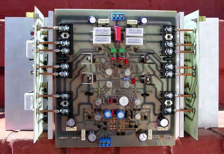
The circuit described on this page is a modification of the original Double Barreled Amplifier. The circuit has been simplified somewhat. The circuit board layout is smaller and much more compact. The driver transistors now mount on the circuit board instead of on external heat sinks. And the circuit has the feedforward compensation that I describe for the Low TIM Amplifier.
The original circuit board for one channel had eight 5-watt resistors on it, one in series with the emitter of each output transistor. On the new layout, four of these have been moved to the heat sink channel where they solder between pins of the transistor sockets. This change not only helps make the circuit board smaller, but it eliminates eight wires between the heat sink and the circuit board. One of the figures below illustrates how these resistors are installed in the heat sink channel.
If you build this amplifier, you must keep the wiring between the heat sinks and the circuit boards as short as possible if you don't want oscillation problems.
When you test the circuit boards before connecting the power transistors, temporarily connect a 10 ohm resistor in series with a 0.1 ufd capacitor from the loudspeaker output to the power supply ground.
Rasmus Haraldseide in Norway has made a YouTube video that shows the amplifier that he and his friend Jonas built.
Here are some pictures that Dennis Cooksey sent me of his amplifier. He has modified the construction to eliminate many wires from the main board to the TO-3 output transistors.
If you print the circuit diagram, first set your print properties for landscape printing. The figures are in Adobe Acrobat format.
In Nov. 2000, I discovered that Adobe Acrobat 4.0 Reader, unlike previous versions, does not print a page to its original size unless you have the right box checked in the Adobe Print Menu. You must verify that the layout and template print to the correct size! The circuit board measures 4 inches by 6 inches. Some of the Adobe Acrobat readers do not print to the original size unless the right boxes in the print menu are checked. For example, there are 4 check boxes in the Acrobat print menu for my HP LaserJet 2100M printer. With the "Print as Image" box checked and the other three unchecked, the layout prints to the correct size. With other printers, it may take some experimentation to obtain the correct setting. After printing, remove the check in the "Print as Image" box. Otherwise, fonts will be printed as images and will not be very clear. The Print Menu for other printers may be different. For example, I have been told that for the HP DeskJet 970 Cxi, you should use the "Picture Mode" rather than the "Page Mode" to get the correct size.
I do not have circuit boards for the Double Barrelled Amplifier. If you wish to build it, you must make your own. Two drawings show the parts layout on the board, one with circuit traces and one without. These are scaled by a factor of 1.5. The other shows the circuit traces only. All layout views are from the component side of the board. You must flip the layout for the foil traces over to obtain the solder side view. The circuit board measures 4 inches by 6 inches. To my knowledge, there are no errors in the layout. If you decide to use it, you should carefully check it for errors because I could have easily made a mistake.
I do not recommend that you make the circuit boards unless you have experience in doing it. A source of materials for making your own printed circuits can be found here. I have been told that their "Press and Peel Blue" product (not the wet stuff they sell) can be used to successfully make boards with traces as narrow as 0.01 inch. The smallest traces on the amplifier layout are 0.03 inch wide. The PnP Blue product is basically a transfer medium that allows you to transfer the toner image from a laser printer directly onto bare copper clad board and then etch it in FeCl3 (ferric chloride).
After you etch the board, the copper should be cleaned with steel wool, lightly coated with solder flux, and then "tinned" with a soldering iron and rosin core solder. Do not use a commercial tinning solution that you dip the board into. It is almost impossible to solder a board that is tinned with one of these products because they corrode very quickly. When you drill the board, you should use the correct size drill bit for the pads. The hole diameters I recommend are: small pads - 0.032 inch, medium pads - 0.040 inch, large pads - 0.059 inch, mounting holes - 0.125 inch. If you do not use a sharp drill bit, you can pull the pads off the board when you drill it.
If you compare the Double Barreled circuit to the Low TIM circuit, you will see a lot of similarity between the two. Indeed, there is a Low TIM Amplifier embedded in the Double Barreled Amplifier. The major difference between the two is that transistors are added in series with those in the Low TIM circuit to form the Double Barreled circuit. By doing this, the voltage across the transistors is decreased so that the power supply voltage can be increased for higher output power.
Basically, the circuit description for the Low TIM Amplifier also applies to the Double Barreled Amplifier. The major difference between the two is the addition of transistors Q22 through Q31. Q22 is connected as a common base stage at the output of Q12. The two transistors form a cascode stage. The base of Q22 connects to the junction of R52 and R54. These two resistors are equal and are connected as a voltage divider between the loudspeaker output and the positive rail. This forces the base voltage of Q22 to float half way between the loudspeaker output voltage and the positive power supply rail. Similarly, Q13 and Q23 form a cascode stage. R53 and R55 force the base of Q23 to float half way between the loudspeaker output voltage and the negative power supply rail. The addition of Q22 and Q23 cause the collector to emitter voltages of Q12 and Q13 to be approximately one-half of what the voltages would be without Q22 and Q23.
Transistors Q24 and Q25 connect in series with the pre-driver transistors Q14 and Q15. The base of Q24 floats half way between the output voltage and the positive rail. The base of Q25 floats half way between the output voltage and the negative rail. The addition of Q24 and Q25 cause the voltages across Q14 and Q15 to be approximately one-half of what they would be without Q24 and Q25. Similarly, transistors Q26 through Q31 cause the voltages across Q16 through Q21 to be approximately one-half of what they would be without Q26 through Q31. By connecting the transistors in series in this way, the rail voltages can be increased for higher output power.
The basic construction details of the Low TIM Amplifier also apply to the Double Barreled Amplifier. There are two short circuit jumper wires that must be soldered on the circuit board. These are marked with a J on the layout. In addition, you must solder a short circuit jumper in place of C6B if you use a non-polar capacitor for C6A. This is explained in the parts list for the Low TIM Amplifier. Because there are eight output transistors, two main heat sinks per channel are required. Q18, Q20, Q28, and Q30 should be mounted on one and Q19, Q21, Q29, and Q31 on the other. Resistors R61 through R64 and wires connecting the collectors of Q18 and Q20 and the collectors of Q19 and Q21 mount on the heat sinks. These connect between lugs on the transistor sockets. The four bias diodes D1 through D4 can be mounted on either heat sink. It is not necessary to divide the diodes between the two heat sinks because both heat sinks will operate at the same temperature. I recommend setting the voltage across Q7, i.e. the voltage between the collectors of Q22 and Q23, so that that amplifier is biased at 120 mA. This will give the same quiescent power dissipation per heat sink as in the Low TIM Amplifier.
After you solder the parts to the circuit board, it is tested using the same procedure specified for the Low TIM circuit board. First, you must solder the short circuit jumper across Q7 and you must solder the 100 ohm 1/4 W resistors from the loudspeaker output to the emitters of Q16 and Q17. If you don't have a bench power supply that puts out plus and minus 85 to 93 V dc, you can test the circuit board at a lower voltage. I would prefer test voltages of at least plus and minus 50 V dc. An option is to connect bench power supplies in series to obtain the plus and minus 85 to 93 V dc. I have routinely connected two 40 V Hewlett Packard power supplies in series with the positive and negative outputs of a Hewlett Packard 50 V dual power supply, and I have never had any problems. To protect the circuit boards, you might want to put a 100 ohm 1/4 W resistor in series with the plus and minus power supply leads for the tests. The current drawn by the circuit should be low enough so that the voltage drop across these resistors is less than 1 V if nothing is wrong on the circuit board. There are 2 ground wires from the circuit board. Both must be connected when testing the boards.
I can't stress how important it is to be careful in testing a circuit board. Even simple errors can cause the loss of many expensive transistors. I always use current limited bench power supplies to test a circuit board before and after connecting the power transistors. I also bias an amplifier using current limited power supplies in place of the amplifier power supply. When I initially power up an amplifier with its own power supply, I always use a Variac variable transformer to slowly increase the ac input voltage from 0 to 120 V rms while observing the amplifier output on an oscilloscope with a sine wave input signal. If I see anything wrong on the oscilloscope, I turn the Variac to zero and try to diagnose the problem using the bench power supply. I never use a load on the amplifier for these tests.
With the following exceptions, the parts for the Double Barreled Amplifier are the same as for the Low TIM Amplifier.
The power supply circuit diagram is the same as for the Low TIM Amplifier. The parts are the same with the following exceptions.
This page is not a publication of the Georgia Institute of Technology and the Georgia Institute of Technology has not edited or examined the content. The author of this page is solely responsible for the content.