
W. Marshall Leach, Jr., Professor
Georgia Institute of Technology
School of Electrical and Computer Engineering
Atlanta, Georgia 30332-0250
Copyright 2000. All rights reserved.
Click here to download an LTSpice file for the amplifier. It was developed by Valerio Maglietta who generously shared it with me.
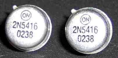 Warning to amplifier builders! Dated 08/14/06. One amplifier builder found that the 2N5416 PNP transistors that he purchased were NPN. I have tested them and verified this. Two of the transistors are shown in the linked photo. They are identified by the letters ON surrounded by a circle, signifying they are products of ON Semiconductor. You can check for a transistor type as follows: Connect an ohmmeter from base to emitter. You should get a low resistance with the positive lead to the base if it is NPN, otherwise it is PNP. With the ohmmeter connected from base to collector, you should get the same result. Repeat the tests with the negative lead connected to the base. The resistances should be reversed. You should get an open circuit from collector to emitter with both polarities of the ohmmeter. Defective transistors usually can be determined with these tests. The transistors should be removed from the circuit for the most reliable results. I have later found that these transistors could be counterfit units made by another company and labeled with the ON Semiconductor name.
PDF of Overall Circuit Diagram
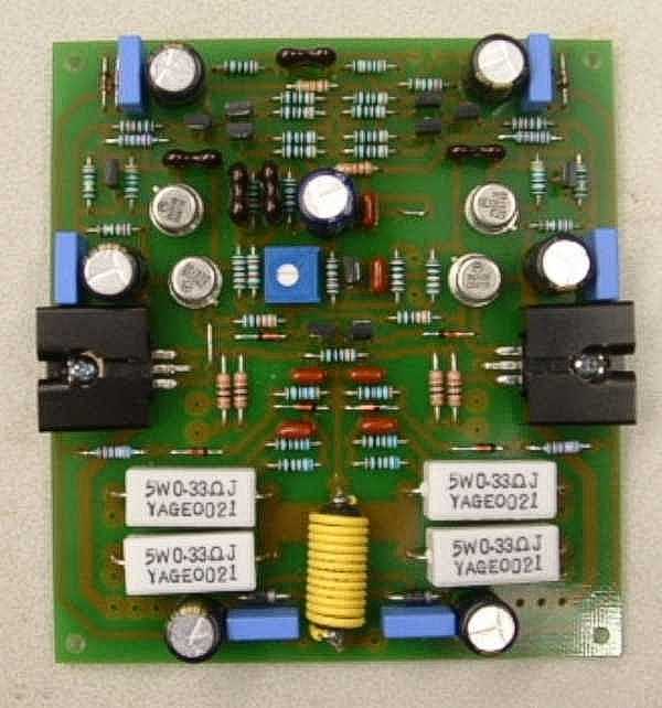
Photograph of assembled circuit board.
The Cascode Diff Amp Input Stage
Parts List and List of Suppliers
Clipping Indicator - Several students who have built the amplifier wanted to add a clipping indicator. I found this circuit in my filing cabinet. It was given to me many years ago. I understand that it was described in an article by Chris Russell in Issue 3 of The Audio Amateur in 1975. We changed some of the resistor values and it seems to work quite well with the amplifier. The two 12 kohm resistors can be changed to vary its sensitivity.
Component Change: R37 through R40 - 680 ohm (changed from 470 on 4/4/2). This change makes the protection circuit less sensitive so that the amplifier can drive more current into lower impedance loads. I made this change after a correspondent told me that he built the amp to use with his home built electrostatic speakers which have a very low impedance. He said the amp sounded distorted. He removed the protection circuit and that solved the problem. He said that he has had no problems with the amp with the protection circuit removed. My original amp had no protection circuit, and I never had any problems with it.
PDF of Circuit board foil pattern and template for drilling heat sinks. The circuit board measures 4 inches by 4.4 inches. There are layouts for both the solder and the component sides of the board. The template for drilling the heat sinks has the holes marked for the power transistors and the bias diodes. You must verify that the layout and template print to the correct size! You do this by verifying that the line at the bottom of the page measures six inches. If it doesn't, you will have to change the print settings for the Adobe reader. Do not use the board layout or heat sink drill template if it doesn't print to the correct size! Thanks to Damir Arbula for cleaning up some printer artifacts that were on my original layout and making the layout for the circuit side of the board.
Layout of parts on the circuit board with the copper traces beneath the board shown.
Layout of parts on the circuit board with the copper traces beneath the board not shown.
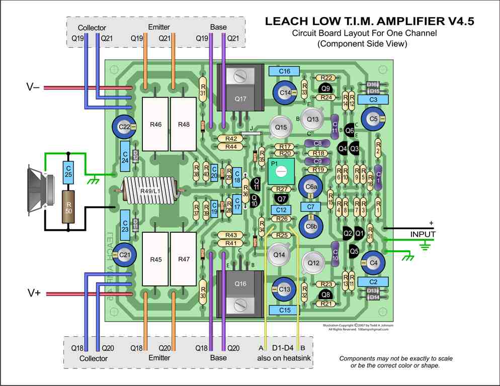
Color layout of parts on the circuit board with the copper traces beneath the board shown. Thanks to amplifier builder Todd Johnson for this!
I used a DOS program called Tango to lay out the amplifier circuit board. The Tango layout and the Gerber files it created are in this zipped folder. Click on the link and save the folder to your computer. I intend to check to see if all of the files are in the directory and add any missing ones, provided I can find them.
Here is a Powerpoint Slide Show sent to me by Bradley Koeppel and Jeff Stout. Bradley is an EE and Jeff is a ME. It shows the constuction of two 5 channel amplifiers, which they built. These are some of the best looking amplifiers I have seen. Here is a picture of the finished front panel of Bradley's amplifier.
Parts Sources and Prices Prepared by Students I am sure many of these prices are out of date. For example, MCM has almost tripled the price for their transistors.
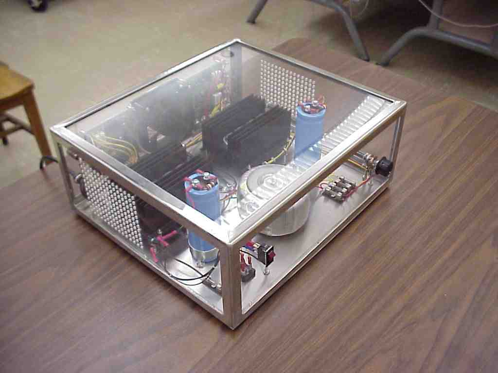
View a picture of student Allen Robinson's amplifier here.
View a picture of student Dan Leverett's amplifier here.
John Mitchell received his amplifier circuit boards in September 2004. In April 2005, he sent me pictures of his work in progress. He said that it was his first electronics project and is a lot of work. He is building his amplifier on aluminum plates and installing it inside a commercial chassis. You can see pictures of his amplifier here.
View an amplifier concept designed by Carl-Fredrik Gustavsen here.
Derek Beamer's Amplifier Page. Derek is in the Toronto area.
Klas Malman's Amplifier Page. Klas lives in Sweden.
The Double Barreled Amplifier Page
Greg's Download Page - A wealth of free software for electronics projects.
I have circuit boards for the amplifier which are fabricated by a local PC board manufacturer. They are pre-drilled for the correct wire sizes and have a solder mask to prevent solder bridges between traces. These are Vers. 4.5 boards which have the hole spacings between two resistors increased by 0.1 inch compared to the Vers. 4.4 boards. If you wish information on these, I can be contacted at
![]()
Please put "Low-TIM PCB" in the subject header of any email that you send to me. I get so many spam emails and emails from our school that sometimes I just don't see inquiries about amplifier circuit boards before my email gets deleted. I apologize if any of your inquiries do not get answered on time.
I do not recommend that you make the circuit boards unless you have experience in doing it. A source of materials for making your own printed circuits can be found here. I have been told that their "Press and Peel Blue" product (not the wet stuff they sell) can be used to successfully make boards with traces as narrow as 0.01 inch. The smallest traces on the amplifier layout are 0.03 inch wide. The PnP Blue product is basically a transfer medium that allows you to transfer the toner image from a laser printer directly onto bare copper clad board and then etch it with FeCl3 (ferric chloride). This is nasty stuff and it should not be disposed of in your drain.
After you etch the board, the copper should be cleaned with steel wool, lightly coated with solder flux, and then "tinned" with a soldering iron and rosin core solder. Do not use a commercial tinning solution that you dip the board into. It is almost impossible to solder a board that is tinned with one of these products because they corrode very quickly. When you drill the board, you should use the correct size drill bit for the pads. The hole diameters on my boards are: small pads - 0.032 inch, medium pads - 0.040 inch, large pads - 0.059 inch, mounting holes - 0.125 inch. If you do not use a sharp drill bit, you can pull the pads off the board when you drill it.
LSR&D and Electronics One amplifier circuit diagrams.
This page is not a publication of the Georgia Institute of Technology and the Georgia Institute of Technology has not edited or examined the content. The author of this page is solely responsible for the content.